About ESA
The European Space Agency (ESA) is Europe’s gateway to space. Its mission is to shape the development of Europe’s space capability and ensure that investment in space continues to deliver benefits to the citizens of Europe and the world.
Highlights


Latest


Space in Member States
Find out more about space activities in our 23 Member States, and understand how ESA works together with their national agencies, institutions and organisations.
 Germany
 Austria
 Belgium
 Denmark
 Spain
Spain
 Estonia
 Finland
 France
 Greece
 Hungary
 Ireland
 Italy
Italy
 Luxembourg
 Norway
 The Netherlands
 Poland
 Portugal
 Czechia
 Romania
 United Kingdom
 Slovenia
 Sweden
 Switzerland
Science & Exploration
Exploring our Solar System and unlocking the secrets of the Universe
Go to topicAstronauts


Latest


Enabling & Support
Making space accessible and developing the technologies for the future
Go to topicLatest


Inner space engineering
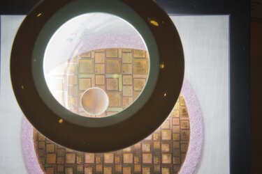
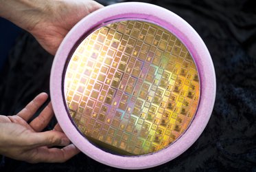
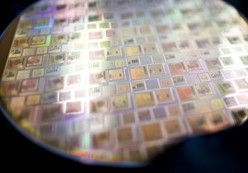
Etched on this wafer of polished silicon are dozens of space-ready integrated circuits ready to be separated into individual chips. These highly intricate items incorporate multiple layers to maximise their functionality, with surface structures smaller in size than many individual viruses.
In the future these circuits are going to be manufactured at still smaller scales: for European space missions to become more capable, the microprocessors that run them need to get more powerful, which means shrinking down the features etched upon them. This is the goal of ESA’s new Ultra Deep Submicron Initiative.
ESA microelectronics engineer Boris Glass is the initiative’s technical officer: “For space missions as much as everything else, it’s the underlying technology that defines performance, which comes down to microelectronics. In everyday life we’re used to Moore’s Law, where microprocessors double in power every 18 to 24 months while also dropping in price. This is because more and more miniaturised transistors can be placed on the same area of semiconductor, down to a few nanometres, or millionths of a millimetre.
“This is talking about the general-purpose microprocessors found in smartphones, computers and other consumer electronics. Billions of chips are manufactured annually. But the space sector has specialised requirements, meaning we often cannot simply make use of those chips as they are, without reworking. And in commercial terms we’re a niche market, requiring tens of thousands of chips at most, rather than many millions.”
Europe’s current LEON5 space-optimised integrated circuit has nodes down to 65 nm scale. ESA’s Ultra Deep Submicron Initiative is targeting nearly an order of magnitude smaller, down to 7 nm.
Boris adds: “While people often think of space technology as always being the cutting edge, that isn’t really the case when it comes to microelectronics. We’re about seven years behind the current state-of-the-art. So this new initiative is essential if we want to take advantage of the latest performance gains, for more powerful and agile future missions and a more competitive space sector – based on sustainable access to new chips with a rapid time to market with no access restrictions.”
The most important difference between the terrestrial and space environments is space radiation. Anything placed in orbit gets randomly bombarded by charged particles or cosmic rays that can randomly flip memory bits, known as Single Effect Events, or cause more lasting damage, such as runaway short circuits known as ‘latch ups’.
Countermeasures to these effects are possible, such as adding in electrical protection to confine some currents or adding redundancy to the chip so that a single bit flip will not irreparably degrade onboard memory. In some cases, multiple memories noting discrepancies get to vote to determine which is the correct value. These countermeasures have to be built into the microprocessors themselves, made available part of the library of building blocks available to integrated circuit designers.
The Ultra Deep Submicron Initiative is being led for ESA by the Sweden-based Frontgrade Gaisler company, which has been active in the field of space-grade microprocessor technology for nearly 25 years.
Frontgrade Gaisler’s General Manager Sandi Habinc comments: “Our consortium’s initial focus is to establish radiation-hardened libraries and intellectual property (IP) cores that will serve as the foundation for highly reliable and efficient integrated circuits. This is a bottom-up approach, starting with the fundamental building blocks needed for developing advanced products. At the same time, we are setting the system requirements such as computational capabilities and interfacing requirements to define the initial products that will come out of the initiative, such as high performance microprocessor.
“For the advanced 7 nm technology we are currently working with a foundry outside Europe, but over time it is expected the same or even more advanced nodes will also be available in Europe as we move forward. It is therefore important that our developments remain generic enough and portable to other manufacturers and foundries, which is a key challenge. Europe is already well-positioned when it comes to advanced packaging, and parallel activities will address the packaging challenges, as well as targeting European electronic design tools.
“It will be a challenge to remove all dependencies when it comes to the design and manufacture of state-of-the-art integrated circuits, so we should therefore focus on the most critical areas. This investment will ensure that Europe remains at the forefront of innovation and autonomy, securing the technology necessary for next-generation space exploration and satellite constellations, including advanced AI and Edge computing.”
This initiative is part of a larger ESA-backed ‘EEE (Electrical, electronic, and electromechanical) Space Components Sovereignty for Europe’ programme, introduced as part of the EU’s European Chips Act, aimed at strengthening the entire European supply chain for space-ready integrated circuits, ranging from design houses to foundries to packagers and test service providers.