Going GaN: novel chips powering space missions
Some of ESA’s most ambitious future missions for telecommunications and Earth observation have only become possible because of a switch to a novel high-power and high-temperature capable semiconductor – sometimes termed the most promising material since silicon. ESA laboratory testing has confirmed the performance of key European-made Gallium Nitride components.
Without knowing it, you already own some Gallium Nitride (GaN) crystals. GaN-based Light Emitting Diodes generate the laser light used to play Blu-Ray discs, provide backlight for modern TV and computer screens and sit within high-efficiency LED light bulbs. The latest slimline chargers for laptop batteries also incorporate GaN-based power converters.

As a ‘wide bandgap’ semiconductor, GaN can operate at much higher voltages and temperatures than traditional materials such as silicon or gallium arsenide. It was first commercially employed in the 1990s as an energy-efficient method of generating blue light.
Today – as silicon-based power devices move towards the limit of their operating temperature, breakdown voltage and power density – GaN is increasingly favoured for Radio Frequency (RF) signal amplification as well as very high power switching systems.
ESA’s ESTEC technology centre in the Netherlands recently oversaw lifetime testing of GaN-based high-power amplifier monolithic microwave integrated circuits (MMICs), the basis of a Dual Solid State Power Amplifier design being developed by SENER in Spain through ESA’s PACIS3 Partnership Project, set to operate aboard a pair of next generation Hisdesat telecom satellites, due to launch in 2023-4.
“These integrated circuits rely on a state of the art 0.25 μm gate length GaN technology from United Monolithic Semiconductors,” comments ESA engineer Václav Valenta who supports various developments of active antenna payloads. “This means the transistor gate terminals are fabricated onto the Gallium Nitride semiconductor chips to a size of 0.25 micrometres – a micrometre being a thousandth of a millimetre.

“Our lifetime-test results demonstrate excellent performance of the selected GaN process. This is good news, since the X-band multibeam active antenna payload under development for these satellites will rely on hundreds of such active GaN elements.”
As well as being indispensable to these new telecom missions, GaN technology also sits at the heart of ESA’s ambitious Biomass satellite. Due to be launched next year, Biomass will deploy a massive 12-m diameter reflector to harness long-wavelength ‘P-band’ radar signals, piercing through forest canopies in order to perform a five-year census of all the trees on Earth. The mission as designed is only made possible by GaN-based RF amplifiers, boosting the transmitted RF signals that are then reflected by Earth’s forests back to the satellite.

Looking further ahead, GaN technology will also serve the planned next generation of Copernicus Sentinel-1 radar satellites, with the potential to reduce the overall size of the spacecraft’s C-band transmit-receive modules while boosting its performance and scientific return.
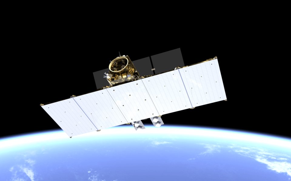
Another forthcoming radar satellite, the high-resolution imaging ROSE-L, will incorporate the highest RF power solid-state transmit-receive modules ever flown in space, thanks to GaN transistors supplying nearly 200 W of power at L-band frequencies. Its active phased array synthetic aperture radar antenna will be the largest planar antenna ever built, measuring an impressive 11 metres by 3.6 metres – roughly the size of 10 ping-pong tables.

“Demonstration and testing is really key to greater adoption of GaN, despite its clear advantages,” adds Václav. “Mission managers tend towards tried and tested technology choices because they desire reliability above all. So rigorous assessment and testing of GaN technology on the ground is essential to understand its potential and limitations, and find solutions making the technology space-compliant in terms of reliability margins. This is what will eventually lead to the mainstream use of GaN technology in space.”
Preparing GaN for space
ESA identified the promise of GaN early. In 2008 the Agency initiated its GaN Reliability Enhancement and Technology Transfer Initiative (GREAT2), bringing together leading research institutes and manufacturing industry to set up an independent European supply chain to manufacture high-quality GaN devices for space applications.

“We could see that Gallium Nitride had the potential to revolutionise communications in space, leading to a five- to ten-fold signal strength and data transmission rates” explains ESA’s Andrew Barnes, overseeing GREAT2.
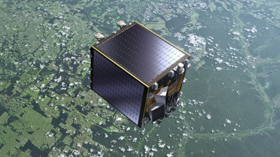
“GaN-based systems also require much less in the way of active cooling, and have a reliability rate that can be measured in decades. As an added inducement for the space sector, they are also inherently radiation resistant. What GREAT2 proceeded to do was establish the performance and reliability of European GaN supply chains, including the flight of the very first GaN-based hardware in space, aboard Proba-V in 2013.”

Earth-observing Proba-V included a GaN amplifier in its X-band communication system, used to downlink images to Earth, which operated faultlessly for more than seven years until the satellite completed its final operations.
Andrew concludes: “The progress made by ESA in the development of GaN technology over the last decade has been paying off and this is demonstrated by multiple examples where GaN is adopted as baseline for critical RF payloads.

“While the mainstream GaN processes used in ESA’s missions are fully qualified or are in the process of obtaining qualification labels, ESA is also investing in development of new advanced GaN technologies for space, working together with the key industrial partners and research centres in Europe to further improve the performance, reach higher frequencies for next generation mm-wave payloads and assure a reliable end-to-end supply chain.”
UMS and OMMIC are the two European commercial sources for advanced GaN and also Gallium Arsenide integrated circuits and qualified semiconductor processes, as specified in ESA’s European Preferred Part list (EPPL).

EEE Space Component Sovereignty for Europe
Can a space mission really be described as European if a majority of its component parts comes from beyond our borders? ESA is proposing the EEE Space Component Sovereignty for Europe initiative for approval by Europe’s space ministers at the Agency’s Council at Ministerial Level at the end of 2022.
Working with industry and key partners, the initiative will reduce the dependence of Europe's space sector on non-European component suppliers, focusing on one of the building blocks of space missions - Electrical, Electronic and Electromechanical (EEE) components. A key aim shall be to develop state-of-art mm-wave GaN processes in Europe.


 Germany
 Austria
 Belgium
 Denmark
 Spain
Spain
 Estonia
 Finland
 France
 Greece
 Hungary
 Ireland
 Italy
Italy
 Luxembourg
 Norway
 The Netherlands
 Poland
 Portugal
 Czechia
 Romania
 United Kingdom
 Slovenia
 Sweden
 Switzerland


